APPLICATIONS
l DWDM Networks
l Fiber channel
l CPRI Rate:2.4576Gb/s
Compliance
l SFP MSA
l SFF-8472
l ROHS
l ITU-T G.694.1
Ordering information
Part No.
Bit Rate
(Gbps)
Laser
(nm)
Distance(km)
Fiber Type
DDMI
Connector
Temp
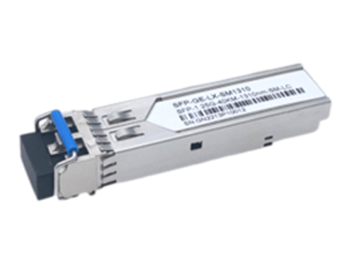
ESGELDxx-Z12C
2.67
C Lane
120
SMF
YES
LC
0℃~70℃
ESGELDxx-Z12I
2.67
C Lane
120
SMF
YES
LC
-40℃~85℃
xx: It’s for Channel
xx
Channel
Frequency
Center Wavelength(nm)
xx
Channel
Frequency
Center Wavelength(nm)
17
C17
191.7
1563.86
40
C40
194
1545.32
18
C18
191.8
1563.05
41
C41
194.1
1544.53
19
C19
191.9
1562.23
42
C42
194.2
1543.73
20
C20
192
1561.41
43
C43
194.3
1542.94
21
C21
192.1
1560.61
44
C44
194.4
1542.14
22
C22
192.2
1559.79
45
C45
194.5
1541.35
23
C23
192.3
1558.98
46
C46
194.6
1540.56
24
C24
192.4
1558.17
47
C47
194.7
1539.77
25
C25
192.5
1557.36
48
C48
194.8
1538.98
26
C26
192.6
1556.55
49
C49
194.9
1538.19
27
C27
192.7
1555.75
50
C50
195
1537.4
28
C28
192.8
1554.94
51
C51
195.1
1536.61
29
C29
192.9
1554.13
52
C52
195.2
1535.82
30
C30
193
1553.33
53
C53
195.3
1535.04
31
C31
193.1
1552.52
54
C54
195.4
1534.25
32
C32
193.2
1551.72
55
C55
195.5
1533.47
33
C33
193.3
1550.92
56
C56
195.6
1532.68
34
C34
193.4
1550.12
57
C57
195.7
1531.9
35
C35
193.5
1549.32
58
C58
195.8
1531.12
36
C36
193.6
1548.51
59
C59
195.9
1530.33
37
C37
193.7
1547.72
60
C60
196
1529.55
38
C38
193.8
1546.92
61
C61
196.1
1528.77
39
C39
193.9
1546.12
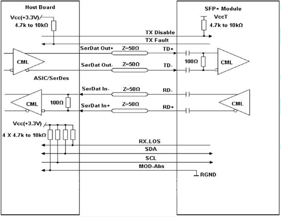
I. Pin Diagram
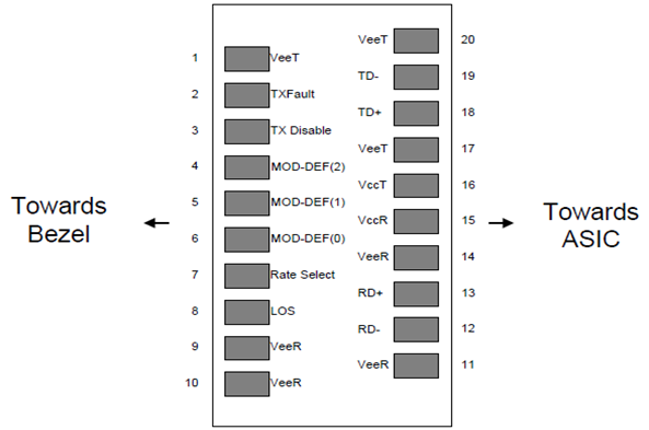
Pinout of Connector Block on Host Board
II. Pin Descriptions
|
Pin |
Symbol |
Name/Description |
Ref. |
|
1 |
VEET |
Transmitter Ground (Common with Receiver Ground) |
1 |
|
2 |
TFAULT |
Transmitter Fault. |
2 |
|
3 |
TDIS |
Transmitter Disable. Laser output disabled on high or open. |
3 |
|
4 |
MOD_DEF(2) |
Module Definition 2. Data line for Serial ID. |
4 |
|
5 |
MOD_DEF(1) |
Module Definition 1. Clock line for Serial ID. |
4 |
|
6 |
MOD_DEF(0) |
Module Definition 0. Grounded within the module. |
4 |
|
7 |
Rate Select |
No connection required |
|
|
8 |
LOS |
Loss of Signal indication. Logic “0” indicates normal operation. |
5 |
|
9 |
VEER |
Receiver Ground (Common with Transmitter Ground) |
|
|
10 |
VEER |
Receiver Ground (Common with Transmitter Ground) |
1 |
|
11 |
VEER |
Receiver Ground (Common with Transmitter Ground) |
1 |
|
12 |
RD- |
Receiver Inverted DATA out (CML). AC Coupled |
|
|
13 |
RD+ |
Receiver Non-inverted DATA out (CML). AC Coupled |
|
|
14 |
VEER |
Receiver Ground (Common with Transmitter Ground) |
1 |
|
15 |
VCCR |
Receiver Power Supply |
|
|
16 |
VCCT |
Transmitter Power Supply |
|
|
17 |
VEET |
Transmitter Ground (Common with Receiver Ground) |
1 |
|
18 |
TD+ |
Transmitter Non-Inverted DATA in. AC Coupled. |
|
|
19 |
TD- |
Transmitter Inverted DATA in. AC Coupled. |
|
|
20 |
VEET |
Transmitter Ground (Common with Receiver Ground) |
1 |
Notes:
1. Circuit ground is internally isolated from chassis ground.
2. TFAULT is an open collector/drain output, which is pulled up with a 4.7kΩ – 10kΩ resistor on the host board, but is grounded inside the SFP+ cable plug.
3. Laser output disabled on TDIS >2.0V or open, enabled on TDIS <0.8V.
4. Mod-Def 0,1,2. These are the module definition pins. They should be pulled up with a 4.7K – 10KΩ resistor on the host board. The pull-up voltage shall be VccT or VccR
Mod-Def 0 is grounded by the module to indicate that the module is present
Mod-Def 1 is the clock line of two wire serial interface for serial ID
Mod-Def 2 is the data line of two wire serial interface for serial ID
5. LOS is open collector output. Should be pulled up with 4.7kΩ – 10kΩ on host board to a voltage between 2.0V and 3.6V. Logic 0 indicates normal operation; logic 1 indicates loss of signal.
III. Absolute Maximum Ratings
|
Parameter |
Symbol |
Min |
Type |
Max |
Unit |
Ref. |
|
Maximum Supply Voltage |
Vcc |
-0.5 |
|
3.6 |
V |
|
|
Storage Temperature |
TS |
-40 |
|
85 |
℃ |
|
|
Case Operating Temperature |
TOP |
0 |
|
70 |
℃ |
Commercial |
|
-40 |
|
85 |
|
Industrial |
||
|
Relative Humidity |
RH |
0 |
|
85 |
% |
1 |
Notes:
1. Non-condensing.
IV. Optical Characteristics (TOP = 0°C to 70°C, VCC = 3.3 ± 5% Volts)
|
Parameter |
Symbol |
Min. |
Typ. |
Max. |
Unit |
Remark |
|
Transmitter |
||||||
|
Center Wavelength Spacing |
λ |
|
100 |
|
Ghz |
|
|
0.8 |
nm |
|
||||
|
Center Wavelength |
λC |
λ±0.1nm |
|
|
||
|
Spectral Width(-20dB) |
Pm |
|
|
1 |
nm |
|
|
Side-mode Suppression Ratio |
SMSR |
30 |
|
|
dB |
|
|
Average Output Power |
Pavg |
2 |
|
7 |
dBm |
|
|
Extinction Ratio |
ER |
8.2 |
|
|
dB |
|
|
Return Loss |
|
12 |
|
|
Db |
|
|
Transmitter OFF Output Power |
Poff |
|
|
-30 |
dBm |
|
|
Transmitter and Dispersion Peralty |
TDP |
|
|
3 |
dB |
|
|
Receiver |
||||||
|
Center Wavelength |
λc |
1260 |
|
1600 |
nm |
|
|
Receiver Sensitivity, Average Power |
|
|
|
-31 |
dBm |
|
|
Receiver Saturation Power |
Psat |
|
|
-8 |
dBm |
|
|
Loss of Signal Assert |
PA |
-45 |
|
|
dBm |
|
|
Loss of Signal De-assert |
PD |
|
|
-32 |
dBm |
|
|
LOS Hysteresis |
PD- PA |
0.5 |
|
|
dB |
|
V. Electrical Characteristics (TOP = 0°C to 70°C, VCC = 3.3 ± 5% Volts)
|
Parameter |
Symbol |
Min |
Type |
Max |
Unit |
Ref. |
|
Supply Voltage |
Vcc |
3.135 |
3.3 |
3.465 |
V |
|
|
Supply Current |
Icc |
|
|
450 |
mA |
|
|
Transmitter |
||||||
|
Input differential impedance |
Rin |
|
100 |
|
|
1 |
|
Differential data input swing |
Vin, pp |
200 |
|
1000 |
mV |
|
|
Transmit Disable Voltage |
VD |
2 |
|
VCC |
V |
|
|
Transmit Enable Voltage |
VEN |
Vee |
|
Vee+0.8 |
V |
|
|
Receiver |
||||||
|
Differential data output swing |
Vout, pp |
350 |
|
700 |
mV |
2 |
|
LOS Fault |
VLOS_fault |
2 |
|
Vcc |
V |
3 |
|
LOS Normal |
VLOS_norm |
Vee |
|
Vee+0.8 |
V |
3 |
|
Power Supply Noise Tolerance |
VCCT/VCCR |
Per SFP MSA |
mVpp |
|
||
Notes:
1. Connected directly to TX data input pins.AC coupling from pins into laser driver IC.
2. Into 100Ω differential termination.
3. Loss Of Signal is LVTTL. Logic 0 indicates normal operation; logic 1 indicates no signal detected.
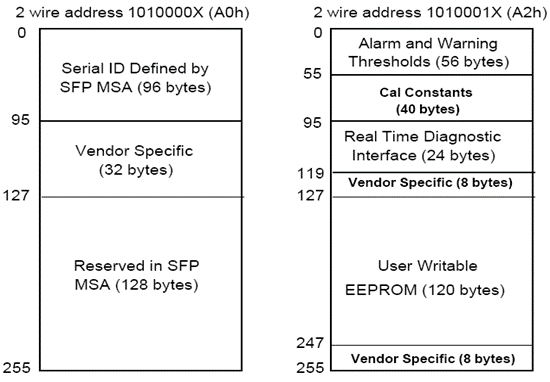
VI. Digital Diagnostic Memory Map
VII. Digital Diagnostic Monitoring Information
|
Parameter |
Unit |
Accuracy |
|
Case Temperature |
℃ |
±3 |
|
Supply Voltage |
V |
±3% |
|
Tx Bias Current |
mA |
±10% |
|
Tx Optical Power |
dB |
±3 |
|
Rx Optical Power |
dB |
±3 |
VIII.Recommended Interface Circuit
IX. Mechanical Dimensions
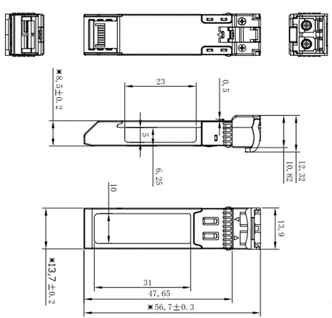
SFP wire mechanical drawing (Unit: mm)
Want to know about this product?
If you are interested in our products and want to know more details,please leave a message here,we will reply you as soon as we can.
 LPGDLB54(B45)-K80C(I)
 LPGDLB53(B35)-K40C(I)
 LPGDLB53(B35)-K20C(I)
 LPGDLB53(B35)-K15C(I)
 LPGDLB53(B35)-K10C(I)
 LPGELCXX-Z12C(E)
 LPGELCXX-K80C(I)
 LPGELCXX-K40C(I)
 LPGDLM85-S55C(I)
 LPGDLB55-K80C(I)

Address : East of 2F, Tianmen Optical Valley Science Park,Qiaoxiang Economic development area,Tianmen, Hubei Province.
Tel : 15012662571
Email : chris.peng@talptech.com
Skype : 15012662571